For decades, integrated circuits have been confined to a veneer on semiconductor chips, with transistors and wiring devices packed ever more densely within this thin sheet. As in-plane shrinkage has become more challenging, however, electronics companies are looking to stack multiple circuit layers vertically to boost speed and functionality, while reducing power consumption and size.
“The performance of a system is not controlled by the individual components, but by the way that you can assemble these different components,” said Paolo Gargini, head of the International Roadmap for Devices and Systems, an IEEE Standards Association Industry Connections program that has supplanted the more device-focused semiconductor roadmap. Over time, stacking will give way to true monolithic growth of three-dimensional (3D) chips for some applications, like memory.
Historically, chips were electrically connected with long, wide metal traces on a printed circuit board, which take a lot of energy and time to charge and discharge. Engineers have long known that stacking chips and connecting them vertically improves both power and speed by reducing the electrical path between them. Memory technology has led the way in exploiting this trick, but the potential benefits affect everything from power-sensitive mobile devices to power-hungry processors in online data centers.
For high-performance computing, “you can save 60%, 90% of the power required, because a lot of it is in communication from a processor and getting access to the memory and doing the compute locally,” said John Knickerbocker of IBM in Yorktown Heights, NY.
Stacking also compactly connects chips made using incompatible processes. At the International Electron Devices Meeting in December, for example, Sony reported sandwiching a logic layer, a DRAM layer, and a CMOS imaging layer in a stack that was only 130 microns thick.

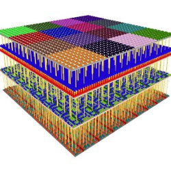
Figure. Artist’s representation of integrated circuits stacked and interconnected by through-chip vias.
A further advantage of combining separate chips is that sensors “include an analog circuit that prefers a higher voltage in many cases. Logic circuits prefer a lower voltage for power consumption and speed,” said Fumiaki Yamada, who worked on the Japanese 3D “Dream Chip” project exploring potential technology for 3D chips, and is now an independent consultant.
Stacking could also be the ultimate way to pack diverse functions into small devices like smart watches, or to drive the nascent “Internet of Things” (IoT). So far, however, many mobile devices still use a more mature technology called package-on-package, which stacks the chips only after they have been packaged. The packages can still be stacked vertically, and they are equipped with an array of solder balls to make many contacts to a common substrate, but the modularity allows manufacturers to design them independently and test them before assembly.
Challenges
True 3D stacking exploits wafer-processing-style tools in service of packaging. One key element is deep etching of uniform vertical channels into a wafer—or even all the way through it. These channels are then filled with metal to form “through-silicon vias” (TSVs) that connect the top and bottom of a chip, “which helps the performance because you don’t have to convey the data to the edge of the chip,” said Yamada. These methods resemble the long-established “flip-chip” face-to-face bonding, but they can extend to many chips.
Another key capability is thinning of wafers to less than the thickness of a human hair, which is useful both for compact stacking and for facilitating drilling holes through them. These sheets, which may be as wide as an entire wafer, then need to be precisely aligned with and bonded to other processed circuits. Yamada notes that reliably handling these thin layers, often after temporarily gluing them to another substrate for handling, is in some ways “still a problem to be solved,” although process engineers have made significant progress.
Stacking also faces other challenges that make it expensive and have so far limited its use. For one thing, the modified structure requires significant changes in design. The array of contacts throughout the active circuitry takes up significant real estate in the middle of the chip that could otherwise be used for transistors. In addition, the different chips in the stack need to be designed with matching pin layouts, which requires a high degree of coordination in the design of the various chips, and limits the manufacturer’s flexibility to modify the layout or use alternative suppliers.
Another major issue is heat removal, which is already a major issue for traditional chips. Combining multiple layers of heat-generating devices, and burying them further from the surface, makes the problem worse. Still, Knickerbocker said, “for low-power applications like some mobile applications and some IoT applications, the power levels are so low that getting the power in and cooling it is not a problem at all,” especially since stacking reduces the total power substantially. For high-performance computing, “even though the power delivery and the cooling challenges go up substantially, there’s still tremendous benefit at the system-performance level to make it worthwhile,” Knickerbocker said, adding that advanced power delivery may be needed, as well as cooling technologies such as flowing liquids through the chip stack or using materials that absorb heat by undergoing a phase transition.
Multiple chips also complicate manufacturing yield, which is critical to the economics of electronics manufacturing. When individual components can be proven functional before assembly, the yield of a multi-chip device can be better than that of a single chip combining the same components. However, without assurance of such “known-good die,” a failure of any layer will require trashing the whole stack.
Memory First
So far, the greatest benefit of 3D chips has been on memory. One reason is that memory consists of identical repeated units, and designers have long taken advantage of the interchangeability of memory blocks to bypass occasional defective ones. (Field-programmable gate arrays have a similar redundancy.) In addition, although heating is a major challenge for stacking of logic chips, in memory chips many transistors are inactive much of the time.
Equally important is the seemingly insatiable demand for memory in all sorts of systems. Indeed, two distinct flavors of vertically stacked DRAM have become important in the last few years. High-bandwidth memory (HBM) has an aggressive champion in AMD, and is already in its second generation, HBM2. A competing technology, Hybrid Memory Cube (HMC), has been developed by Micron. Although there are important differences, both feature very high data rates with over 1,000 or more connections between layers. “For the HBM stacks, the density of the interconnect is now down at like 55μm pitch between connections,” Knickerbocker said.
In this rapidly evolving field, stacking is not the only route manufacturers are exploring for 3D memory, however. Samsung, for example, in addition to its HBM products, has developed a monolithic flash-memory technology called V-NAND, which features strings of dozens of floating gate transistors connected vertically in series along deep etched trenches refilled with silicon, grown over a wafer of control and sensing circuitry.
Micron also has teamed with Intel to develop their own monolithic multilayer flash memory. Although they announced an end to this collaboration in January, the two companies are still collaborating on different monolithic technology, a multilayer resistive memory called 3D-XPoint.
Arms Race
In a more general stacking configuration, combining different types of chip remains challenging. “You’ve got to have the design, you’ve got to have the assembly, you’ve got to have either the same die size or thin chips are hanging out. It’s not so easy,” Knickerbocker cautions. As an intermediate step, “a lot of people over the past five or years have been using what’s called 2.5D, like a silicon interposer, and put multiples of these chips side by side, or some combination of chip stacks and chips next to them,” he said. “You can get lots and lots of connections for adjacent chips in a way that allows that product to be rolled out very quickly without doing the design consistency across many different technologies that go into a full chip stack.”
For example, Nvidia’s latest devices for artificial intelligence applications combine a high-density interconnect on a silicon interposer wafer with HBM memory stacks close to their graphics processor unit (GPU). “That’s a good start,” Knickerbocker said, “but I still think 3D and full chip stacking for many applications will give the best and highest performance at the system level.”
On the other hand, stacking will always be competing with the approach of growing new devices on a wafer during fabrication, but it is hard to develop a monolithic process that does not disrupt the layers below. “Packaging is a shortcut,” said Gargini, who oversaw many generations of this arms race during his decades in technology development at Intel, including the first integration of modest cache memories onto the same die with a processor. “The packaging side buys you performance a couple of generations ahead of technology, then the monolithic part catches up,” Gargini said. “At each point in time, you take the best trade-off between cost and performance.”
In the end, customers care more about the price, performance, and size of the entire packaged device than about how many components are in it or how it is assembled inside. As long as advanced packaging, whether by stacking or other means, provides an advantage, “these companies are absolutely ready to do this stuff,” Gargini said. “They have had these capabilities for a long time.”
 Further Reading
Lapedus, M.
A New Memory Contender?, Semiconductor Engineering, January 2, 2018, http://bit.ly/2DbliT2
Kondo, K., Kada, M., and Takahashi, K. (Eds.)
Three-Dimensional Integration of Semiconductors, Springer International Publishing, 2015, http://bit.ly/2G6uXxd
3D Stacked Memory: Patent Landscape Analysis Lexinnova Technologies LLC, http://bit.ly/2tuC0Ny


Join the Discussion (0)
Become a Member or Sign In to Post a Comment