At the International Symposium of Conference of Physical Design (ISPD ’16) held in early April in Santa Rosa, CA, Intel’s Kevin X. Zhang, vice president of the company’s Technology and Manufacturing Group and director of advanced design in logic technology development, discussed Intel’s processor development from the 90-to-22-nanometer-size node, as well as its plans to scale down further to 14-nanometer, 10-nanometer, 7-nanometer, and 5-nanometer sizes circa 2020.
As a keynoter for the annual event sponsored by ACM’s Special Interest Group on Design Automation (SIGDA) with technical co-sponsorship from the IEEE Circuits and Systems Society (CAS), Zhang said Intel was keeping Moore’s Law alive through the introduction of the world’s first Fin Field Effect (FinFET) transistor at the 22-nanometer size–the pinnacle of Zhang’s career while in the trenches of process development at Intel. Zhang has been promoted to an Intel Fellow, allowing him to peer into the future of microchip technology to define the path that, he hopes, will keep Intel the top semiconductor maker worldwide.
Zhang’s new mission at Intel is to introduce new materials and transistor architectures to surround the existing complimentary metal oxide semiconductors (CMOS) cores (as many as 72 per chip) to produce Intel’s next generation of processors.
In his ISPD keynote, Zhang provided details including listing the type of new materials Intel was considering to its CMOS cores, including on-chip nonvolatile magnetic memory technologies (such as MRAMs), the introduction of gallium nitride transistors for high-power input/output (I/O), the addition of quantum bits (qubits) for acceleration and uncrackable encryption, and more.
IBM vs. Intel
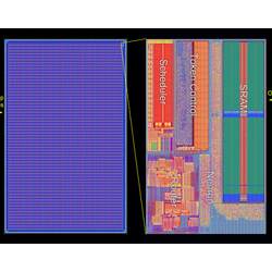
IBM revealed new details about its very different path from Intel, in which it is creating brain-like neuromorphic computer chips called TrueNorth in the paper "Design and Tool Flow of IBM’s TrueNorth: An Ultra-Low Power Programmable Neurosynaptic Chip with 1 Million Neurons" by Filipp A. Akopyan, Low Power Neuromorphic Circuit designer at IBM Research.
TrueNorth is "a 65mW brain-inspired processor that implements a non-von Neumann, parallel, distributed, event-driven, modular, scalable, defect-tolerant architecture," according to the paper’s abstract. The chip houses a 64-by-64 array of neurosynaptic cores (4,096 in total), with 1 million digital artificial neurons (the brain’s processing cores) and 256 million synapses (the brain’s memories) per chip. Amazingly, a gigantic 5.4-billion-transistor TrueNorth implementation consumes only 70 miliwatts of power (an Intel chip of similar size would consume upwards of 100 watts).
The key to TrueNorth’s ultra-low power consumption is that it is modeled on the human brain, which consumes no power except when a neuron collects enough energy from its inputs (called dendrites) and fires a binary pulse (called a spike) down its output (called an axon) to communicate its excited state to the neurons attached to its axon. Since this happens in an asynchronous manner that averages about 10Hz (compare to 3GHz to 5GHz for Intel’s processors), TrueNorth chips can solve supercomputer-caliber problems while consuming milliwatts, instead of the kilowatts supercomputers typically require.
According to Akopyan, the TrueNorth chipset is available on a single-chip board, a 16-chip board, and a 256-chip server-like enclosure, with plans for 1024-chip and 4096-chip models. Software-wise, however, TrueNorth does not learn its algorithms on-chip, but rather an IBM supercomputer is used to perform a perfect simulation during learning, which is then used to configure TrueNorth to solve that problem.
"We do all the learning off-line in just a few seconds on the fly, then download the necessary configuration data into the TrueNorth chips," Akopyan said. "We have already had reference boards at several beta-sites for testing, and we already have a customer, Lawrence Livermore National Laboratories, which is the first customer to allow us to use their name."
Synopsys Roadmap
Silicon transistors will progress from today’s most-advanced 14-nanometer size to 10-, 8-, 5-, 3-, 2- and 1-nanometer-sized nodes, despite those that say Moore’s Law is dead, according to Antun Domic, executive vice president and general manager of the Design Group at Synopsys, who said, "Moore’s Law is alive and well, but a new law has arisen: the number of people saying Moore’s Law is ending doubles every two years."
Domic spoke mostly about the electronic design automation (EDA) tool improvements needed to handle the trillion-transistor chips of the future, while his colleague, Synopsis scientist Victor Moroz, offered hardware reasons for why Moore’s Law will not end any time soon. Moroz said Moore’s Law will extend at least until 2043, when there will be only one atom per transistor. He also predicted the imminent demise of the FinFET transistor and a complete industry switchover to nanowire transistors, which can be scaled down to the atomic level.
According to Moroz, many new transistor architectures are being proposed which will not work for the long run, including fully-depleted silicon-on-oxide transistors (promoted by Soitec), elongated FinFETs (promoted by Intel/Samsung/TSMC) and a switch to gallium-arsenide (GaAs) transistors (promoted by IBM). Moroz cited insurmountable problems ahead for each of these technologies, offering the simple silicon nanowire as a universal solution.
"Silicon nanowires can be scaled down to almost any size, they are more reliable and will become the favorite transistor architecture as we approach the atomic scale," said Moroz.
R. Colin Johnson is a Kyoto Prize Fellow who has worked as a technology journalist for two decades.


Join the Discussion (0)
Become a Member or Sign In to Post a Comment