It is easy to overlook the role lithography plays in developing digital technologies. Every year, new and more advanced integrated circuits appear, pushing computing capabilities to more advanced levels. Typically, the focus is on what these devices can do, in areas like supercomputing, artificial intelligence (AI), and wireless communications, for example. Yet, behind the curtain is the technology that makes all of this possible.
Lithography—which at its most basic level refers to a photography-like process that uses light to imprint images on a suitable substrate, such as a thin film—is at the foundation of modern computing and electronics. Ongoing breakthroughs in the field have produced ever more advanced integrated circuits capable of handling a dizzying array of tasks. This includes the microprocessors and solid-state memory that power today’s electronics.
Yet, lithography has reached a crucial crossroads. Like many areas of computing, it is becoming more difficult to eke out performance gains using existing technologies and methods. For example, innovations tied to the most widely used technology, extreme ultraviolet (EUV) lithography—invented by Netherlands-based ASML, which is the sole supplier of equipment to accomplish this—have slowed. This has set the industry on a chase to find new ways to keep the advancements coming—and a new generation of computing devices operating.
One such breakthrough came in October 2023,a when Canon chairman and CEO Fujio Mitarai introduced a sophisticated nanoimprint lithography system. He labeled the technology a “game changer” and predicted nanoimprint would play an important role in the future of lithography. Although Canon faces obstacles associated with scaling up the technology commercially while reducing error rates, nanoimprint is poised to make a significant mark.
The stakes couldn’t be higher, and how things play out will impact everything from smartphones and Internet of Things (IoT) devices to autonomous vehicles and cloud computing. Moore’s Law, which asserts that the cost per transistor halves every two years, is slowing and there’s hope that continuing breakthroughs in lithography can keep it on course.
“Semiconductor lithography has managed to keep Moore’s Law alive, thanks to scientific and engineering innovations on multiple fronts across the lithography spectrum,” said Ricardo Ruiz, director of the Center for High Precision Patterning Science (CHiPPS)b at Lawrence Berkeley National Laboratory.
A Changing Image
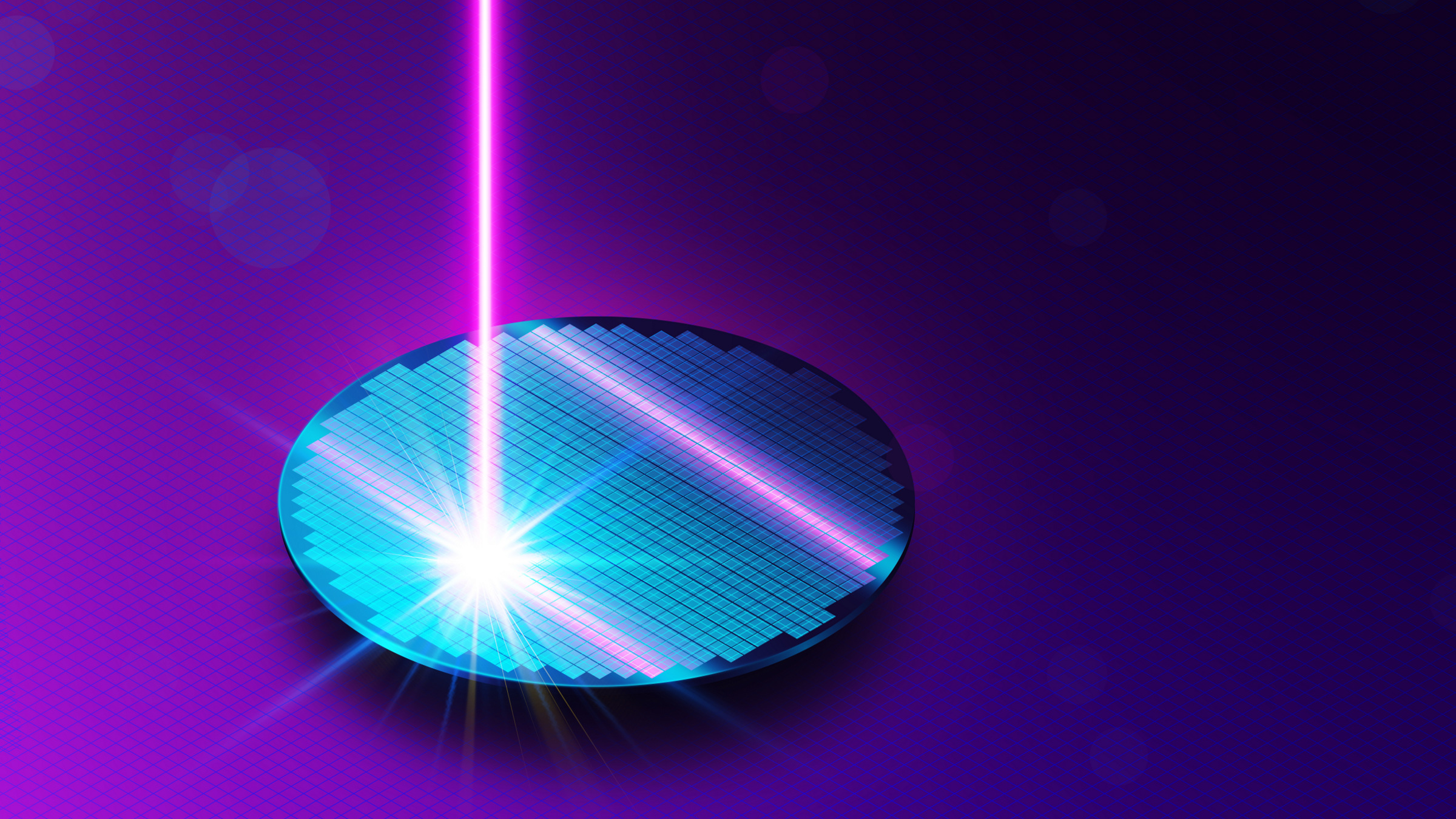
Virtually all of today’s semiconductors—including the chips that power smartphones, smart TVs, PCs, and datacenters—rely on older Deep Ultraviolet (DUV)c technology or Extreme Ultraviolet (EUV) lithography, also known as EUVL systems.d The former produces circuits at a scale down to 40 nanometers, while the latter uses CO2 laser-produced plasma light to enable a scale of 20 nanometers and smaller using a light wavelength of 13.5 nanometers. Both methods work by coating selected regions of an integrated circuit wafer with a photosensitive material using a “mask” and then carefully exposing them to light. This “etches” the desired circuitry onto the wafer that is used to fabricate integrated circuits.
DUV and EUV are complementary; the technologies often coexist on the same circuit or chip. “If you are producing extremely complex chips, they might include 50 billion transistors and interconnects made of tens of layers,” said Harry Levinson, an independent industry consultant and principal at HJL Lithography. “Within a single chip, there may be a need for ultra-small features in one layer but not in another layer. This means it’s possible to use older and less-expensive DUV for some layers of a chip design, but EUV in others.”
Nevertheless, the desire for smaller, faster, more energy-efficient circuits has catapulted EUV lithography into the spotlight. Introduced commercially in 2019 by chip makers TSMC and Samsung using EUV tools from Netherlands-based ASML, the technology introduced a nearly 10x reduction in wavelength from the previous 193 nanometers, thus allowing far more intricate circuitry. Today, ASML controls approximately 90% of the DUV and EUV lithography markets.e Former industry leaders such as Canon and Nikon have taken a back seat and watched their market shares shrink.
Over the last few years, researchers have continued to explore ways to boost lithographic density by incorporating new patterning materials, including high-resolution metal-oxide resists, and developing techniques that incorporate self-assembling polymers at nanoscale. Anthony Yen, vice president and head of the Technology Development Center at ASML, said current research revolves around three key axes: “Shorter wavelength of the light, higher numerical aperture through more advanced optics, and a slew of techniques related to advanced mask designs, advanced mask illumination, and new resist formulations.”
ASML also has pushed EUV technology forward by combining hardware and software within a single system. Meanwhile, Lawrence Berkeley and other research labs continue to explore materials, techniques, and methods to push the field forward. This includes studying advanced self-assembling materials designed to work specifically with EUV radiationf and ways to introduce atomic-level precision that could shrink chip fabrication to 7 nanometers using EUV lithography, Ruiz said.
Researchers also are eying other lithography techniques for applications other than the patterning of high-density digital integrated circuits. For example, electron beam lithography can be used for making the master patterns—photomasks—used in DUV and EUV lithography, and it plays an important role in research and development.
Another technique is nanoimprint lithography, on which Canon is now focused. “These technologies are useful, even if not for patterning wafers in the high-volume manufacturing of integrated circuits,” Levinson explained.
Making an Impression
Canon’s foray into nanoimprint lithography—a project that has spanned more than a decade—takes direct aim at EUV lithography. Its FPA-1200NZ2C nanoimprint lithography system currently supports single-patterning of features with a minimum linewidth of 14 nanometers.g This contributes to lower semiconductor process cost of ownership, Canon says. The technology also allows chip engineers to pattern complex 2-dimensional or 3-dimensional features in a single imprint step. The resulting design freedom is valuable for applications such as logic, memory, AI acceleration, and high-resolution fabrication of head-mounted displays.
Nanoimprinting taps Canon’s expertise in inkjet printing and optical technologies. The system dispenses strategically placed photosensitive resins onto semiconductor wafers, and then depresses high-fidelity etched masks into the resin. After curing by UV light, the mask and wafer are separated, and a high-resolution replica of the mask pattern is transferred to the wafer. The entire wafer is subsequently filled with nanoimprinted patterns through a step-and-repeat process. The technology also includes a novel alignment system that provides nanometer-scale alignment accuracy between mask and wafer patterns.
The breakthrough makes it possible to print ultra-fine circuits at a much lower price point. As a result, manufacturers could find nanoimprint technology valuable for producing highly specialized devices in smaller volumes. This includes more affordable high-contrast micro-OLED panels commonly used for head-mounted displays, as well as various types of communication devices, biosensors, and batteries.
A fundamental shift is taking place in the lithography space, said Doug Shelton, a senior member of the technical staff for product marketing at Canon USA Inc. “Circuit-scaling has become less attractive and has motivated the industry to develop alternative technologies that complement lithography as key drivers for semiconductor innovation.” Shelton believes advanced packaging technology will fuel further advances in chiplets—the integration of multiple chips on a single high-density package. “These will likely become part of future high-performance computing systems,” he said.
Not surprisingly, ASML isn’t resting on its image. For now, it remains the only company capable of manufacturing lithography systems in the single-digital nanometer range, and the company continues to roll out technology innovations, including the use of AI and algorithmic manufacturing methods that produce smaller and more powerful chips free of defects. This year, ASML will begin shipping a next-generation EUV system with a higher numerical aperture for the 2-nanometer node, up from the current 7-nanometer node. This will produce even more detailed circuits. “We do not see other lithographic technologies that can replace EUV lithography in high-volume manufacturing,” Yen said.
Image Is Everything
Future advances in lithography may not occur at the same rate as in years past, but they remain important. Yen said ASML also is focused on eking out advances in new types of photomasks and different types of photoresists, while expanding leading-edge lithography into additional areas, such as dynamic random acc3ess memory (DRAM). The Berkeley Lab, meanwhile, hopes to gain a better fundamental understanding of patterning materials. For example, it is currently developing a suite of characterization and metrology techniques for EUV photoresists. This includes resonant soft x-ray scattering (RSoXS), electron spectroscopy and tomography and other critical in-situ metrology capabilities.
CHiPPS is also focused on developing next-generation EUVL and hardware and resist materials that would introduce far more advanced high-NA EUV and potential -hyper-NA EUV technologies. Further discoveries hinge heavily on a couple of areas, Ruiz said. “The first is on efficiently harnessing high-energy photons to perform selective chemical reactions that can be leveraged for atomically precise patterning at the nanoscale. And the second is mitigating stochastic effects, such as the variability that arises from photon-, atomic-, and molecular-scale variations that ultimately limit sub-nanometer-level precision.”
Materials science may offer ways to get around slowing advances in the field, Levinson said. “There are quite a few materials that show promise—and breakthroughs often take place in unexpected ways.” However, for now, “Many of these technologies remain extremely speculative and unproven.” In addition, Levinson believes the next frontier of chip technology will address power consumption through improved circuit designs, better transistor engineering, and AI. “It’s possible to shrink things only so far before we reach the physical limits of transistors and lithography, perhaps as early as the 2030s,” he said.
Ruiz concurs that a heavy emphasis on research is warranted: “All the applications at the forefront of computing, including high-performance computing, datacenters, mobile devices, automobiles, AI acceleration, and more, stand to benefit from the higher speeds and increased densities enabled by improved lithography.”


Join the Discussion (0)
Become a Member or Sign In to Post a Comment