
Field-programmable gate arrays (FPGAs) are remarkably versatile. They are used in a wide variety of applications and industries where use of application-specific integrated circuits (ASICs) is less economically feasible. Despite the area, cost, and power challenges designers face when integrating FPGAs into devices, they provide significant security and performance benefits. Many of these benefits can be realized in client compute hardware such as laptops, tablets, and smartphones.
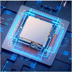
An FPGA is an integrated circuit (IC) composed of configurable logic blocks (CLBs) connected via programmable interconnects (Figure 1);22 it can be configured to desired application or functionality requirements after having been manufactured (hence, field-programmable). In contrast, an ASIC cannot be modified or changed after manufacturing. Examples are a CPU, GPU, or SoC (system on a chip).

Figure 1. Xilinx Spartan-3A FPGA.
Hardware designers use hardware description languages (HDLs) such as VHDL or Verilog to describe the structure and/or behavior of the logic elements within the FPGA. Electronic design automation (EDA) tools are then used to synthesize the design and generate the FPGA configuration, often referred to as a bitstream; finally, the bitstream is applied to the FPGA. (This explanation is a drastic oversimplification and should serve only as a rudimentary description of FPGAs.)
The world’s largest FPGA manufacturers are Xilinx, recently acquired by Advanced Micro Devices (AMD), and Intel (formerly Altera, which Intel acquired in 2015). As of 2019, the FPGA market size was valued at $9 billion and is expected to reach $14.2 billion by 2025.8
Despite their versatility and heavy use in a variety of applications, FPGAs are notoriously absent from modern client compute hardware (for example, laptops, smartphones, desktops, and tablets). This article examines the challenges and benefits of using FPGAs in client compute hardware.
Current Applications
FPGAs are commonly used in the early stages of hardware design for rapid prototyping, testing, and development because they can be reconfigured at will. Otherwise, designers would have to send their designs to the foundry to be fabricated every time they were updated or modified; this can be time-consuming and costly. Other common applications include those in aerospace and defense (for example, avionics and missile defense systems), audio and video (digital signal processing, encoding, and decoding), medical (ultrasound and x-ray), and various other markets and industries.
FPGAs are also commonly used in cloud and datacenter applications. Microsoft’s Azure SmartNIC is a network card that uses an FPGA to accelerate network performance (lower latency and higher throughput) of the virtual machines offered through its Azure cloud service.7 Amazon Web Services (AWS) offers virtual machines with FP-GAs that developers can use to accelerate their applications.20 For those who wish to run applications in their own datacenters, FPGAs are available as Peripheral Component Interconnect Express (PCIe) add-in cards that can be integrated into new or existing servers; developers can then use them to accelerate their applications.19
Generally speaking, FPGAs are found wherever the volume of units or devices produced is relatively small such that it is more economical to use an FPGA for the application than it is to design and fabricate an ASIC.
Challenges
A variety of nontrivial challenges arise when hardware designers integrate FPGAs in client compute devices. These include area (the amount of space on the printed circuit board that the FPGA will occupy), power consumption, and cost.
Area. At Macworld 2008, Steve Jobs, the CEO of Apple at the time, unveiled the MacBook Air, a laptop computer so thin and light it could fit inside an envelope. At the time, the consumer electronics industry had already been moving toward thinner and lighter devices; it was a natural progression. The MacBook Air, however, was so radically thin and light in comparison to its competition that OEMs had no choice but to press the fast-forward button and make size and weight of their devices a priority in order to remain competitive. To this day, size and weight remain a priority for both hardware designers and consumers of client compute devices.
In comparison to ASICs, FPGAs use more area for the equivalent amount of logic and functionality implementation. The units of measure in question are square millimeters (mm2), which may seem negligible at first glance; in modern device design, however, every micron counts.
Cost. From a bill of materials (BOM) perspective, FPGAs are more costly than ASICs. Depending on the target audience and market, such as consumer electronics, the OEM or system designer must deal with tight margins and specific price targets for a product to be economically feasible and sell at worthwhile volumes. Increasing the BOM by introducing an FPGA may cause the overall target price of the product or system to be outside of an acceptable range.
Power. FPGAs consume more power than ASICs.12 In large, complex systems (where power consumption is either not as much of a constraint or where the increase in power from one or multiple FPGAs is negligible) power consumption might not be much of a concern. In client compute devices, however, power consumption is given high priority in overall system design. Lower total cost of ownership (TCO) and increased battery life (in the context of mobile devices) are highly desirable characteristics in the consumer electronics world.
Benefits
Integrating FPGAs into client compute hardware realizes a variety of benefits.18 They can be used to accelerate otherwise-expensive operations, which, in turn, can lead to increased performance and power efficiency. Their reconfigurable nature lets hardware that has already been deployed be updated throughout its life cycle (for example, fix a security issue or improve performance). If done carefully, choosing to implement a particular function in hardware by means of an FPGA has the potential to increase the overall security of a device.
Hardware acceleration. Hardware acceleration and heterogeneous compute architectures are becoming more prevalent. In other words, use the right tool for the job; not all workloads are well-suited for one particular type of hardware (for example, CPUs or GPUs).
There are several examples of this in modern compute devices:
- Apple’s M1 SoC features dedicated neural network hardware known as the Neural Engine; it’s used for Face ID, Animoji, and other machine-learning workloads/tasks. While these tasks could be processed on the CPU or GPU, using dedicated hardware gains significant power efficiency and performance benefits.
- ARM’s big.LITTLE architecture combines two types of CPU cores: those designed for higher performance and those designed for power efficiency; certain tasks and workloads are more suited to different power and performance profiles.
- The AES-NI (Advanced Encryption Standard New Instructions) accelerate AES encryption and decryption operations. Given how frequently these operations are performed, accelerating them in hardware brings power efficiency and performance benefits.
FPGAs can be used to accelerate specific workloads in situations where such workloads are significant enough to realize performance and/or power benefits. OEMs and system designers may favor an FPGA over an ASIC for these reasons:
- As previously mentioned, it is not economically feasible to design and manufacture an ASIC.
- No such hardware exists to accelerate such a workload.
- The desired integration or functionality of the accelerator does not exist using available hardware.
Patching and updates. As previously discussed, a major benefit of using an FPGA is its ability to be reconfigured once deployed. In practice, this means that hardware can be modified or updated over time. This benefits both designers (for example, less manufacturing overhead) and consumers (for example, no confusion over which product to buy or product obsolescence). For example, if accelerating the encode or decode of a particular audio or video codec, the implementation may change or be updated over time.
Another major benefit is the ability to fix or patch security vulnerabilities discovered over time.6 ASICs suffer from the inability to be modified after being manufactured; Spectre and Meltdown, and variations of each, are glaring examples of how crippling a hardware vulnerability can be. The ability to patch hardware cannot be overstated.
FPGAs are found wherever the volume of units or devices produced is relatively small such that it is more economical to use an FPGA for the application than it is to design and fabricate an ASIC.
Enhanced security. Before diving into this section, let’s make two things crystal clear:
- There is no such thing as a perfectly secure system. Philosophically, we, as human beings, are imperfect, and the systems we design and use are inherently imperfect.
- Hardware is not inherently more secure than software. If something is implemented in hardware instead of software or firmware, that does not magically make it more secure.
Despite these two sobering points, implementing a particular function in hardware can improve the overall security of a system. For example:
- The SoC used in the Microsoft Xbox One video-game console, illustrated in Figure 2, has a dedicated hardware PIN used to access secret keys for decryption of sensitive data.13 This ensures the keys are never exposed to software or any other part of the system at any point in time.

Figure 2. High-level depiction of the Xbox One X SoC architecture.
- Apple’s storage architecture in systems that use the Apple T2 SoC has both security and performance benefits compared with devices that use more-conventional storage architectures. As illustrated in Figure 3, the SoC sits in the direct memory access (DMA) path between the CPU and the nonvolatile storage.3 This keeps secret keys used to encrypt and decrypt data out of the hands of the rest of the system (for example, the CPU and any software running on it). An additional benefit of this architecture is enhanced performance; the T2 SoC acts as the storage controller that performs all reads and writes to the NAND flash modules.

Figure 3. Storage architecture on Apple devices that use the T2 SoC.
- Biometric authentication, the way that body measurements such as fingerprints or faces are used to authenticate, is becoming more and more prevalent because it is stronger than password authentication. Processing biometric information raises significant privacy and security concerns, such as how that information is being stored, processed, and handled. Early biometric authentication mechanisms processed an individual’s biometric information directly on the host device (that is, in software on the CPU); this means that biometric information is now exposed to software and various components within the system. Modern biometric authentication mechanisms, such as the Synaptics FS760016 illustrated in Figure 4, store, process, and handle all biometric information on a single SoC; this means that biometric information is never exposed to the host operating system, CPU, or any other hardware or software component of the system.

Figure 4. Synaptcs FS7600 biometric authentication SoC.
Choosing to implement certain functions of a system’s architecture can thus yield security benefits. FPGAs offer the same potential benefits as an ASIC would with the added benefit of being reconfigured throughout the system’s life cycle. If security is a priority in system design (which it should be), then being prepared when security vulnerabilities are found and being able to remediate them (perhaps by means of an update to the FPGA) should also be a priority.
Putting It All Together
This section focuses on a scenario in which an FPGA is used instead of an ASIC to demonstrate the practicality of integrating programmable logic into client compute hardware designs. In this scenario, a solid-state storage device (SSD) inside a client compute device uses an FPGA to implement the functions of the storage controller; Figure 5 is a high-level depiction of the SSD’s architecture. The FPGA will be used to implement:

Figure 5. Storage device architecture used in a compute device.
- Crypto engine. Performs all encryption/decryption operations on data that is read/written.
- DRAM controller. Interfaces with the DRAM (typically used as a cache).
- NAND controller. Interfaces with the NAND flash modules within the storage device.
- Processor. Houses the core logic of the storage device.
- Host interface controller. Interfaces with the host (for example, laptop, desktop, smartphone, and tablet) via Nonvolatile Memory Host Controller Interface Specification (NVMe), or Serial ATA (SATA), Serial Attached SCSI (SAS), and so on.
It’s important to note that many of the points being made in this section would apply if an FPGA were used in other ways (for example, audio/video, encode/decode, facial recognition).
Area. A standard M.2 2280 SSD measures 22mm x 80mm, a total of 1,760mm2. This form factor is a single, rigid piece of hardware. While an FPGA required to implement the logic described in this hypothetical SSD would be larger than most storage controller ASICs found on commercial SSDs, it would be advantageous to the designer to break apart the components. Rather than cram everything onto a single M.2 2280 form factor, why not take advantage of the space of the PCB (printed circuit board) and spread the components out?
There is no such thing as a perfectly secure system. Philosophically, we, as human beings, are imperfect, and the systems we design and use are inherently imperfect.
As shown in Figure 6, the 13-inch MacBook Pro from 2020 uses an irregularly shaped PCB to take advantage of every square millimeter available in the chassis. Components are placed throughout, rather than using larger, rigid components such as M.2 SSDs. (Note the placement of the NAND flash modules and the Apple M1 SoC.)

Figure 6. Shape/layout of the late 2020 13-inch Macbook Pro PCB.
Figure 7 shows an example layout of the components of the SSD distributed throughout the PCB rather than lumped together in an M.2 2280 form factor. An M.2 SSD would take up a considerable amount of space on the PCB and make it more challenging to fit other components. Breaking the components apart and spreading them across the PCB makes better use of the space. This is a fair compromise to ensure that size/space requirements are met.

Figure 7. Example layout of the components of the SSD.
Power and performance. An Intel Optane 905P SSD consumes 9.35W when active and 2.52W when idle; it has a sequential read and write bandwidth of 2,600MB/s and 2,200MB/s, respectively.9 Ruan et al. have demonstrated that an SSD design similar to the one proposed here (an FPGA-accelerated SSD) consumes around 10W active and realizes an average 12x performance increase compared with an SSD that uses a quad-core ARM CPU as the storage controller.15 While there is an increase in power consumed, there is also a significant increase in performance.
IP theft. Reverse engineering an IC can reveal its structure, design, and functionality. A common protection against this is IC camouflaging, but this brings with it significant area, power, and delay overhead.14 TechInsights offers professional services to reverse engineer ICs,17 and Degate even offers software products that can be used to perform reverse engineering of ICs.5 While reverse engineering is commonly performed for legitimate reasons, a malicious entity could reverse engineer an IC to steal/pirate the design. When attempting to do so on an FPGA IC, however, a malicious entity could learn of only the FPGA itself and not the logic or IP implemented.
It is worth noting that FPGAs are potentially exposed to other malicious attacks and/or piracy through manipulation and/or reverse engineering of the bitstream. The bitstream can be manipulated such that when it is loaded into the FPGA, it causes unwanted behavior; it can also potentially be extracted and reverse engineered. While this may seem alarming, both commercial4,23 and academic10 methods are available for protecting the bitstream.
Cost. For end users of a compute device using an FPGA, overall TCO is reduced. Throughout the life cycle of the device, as implementations of the IP blocks in the SSD improve (for example, efficiency and security) and the FPGA configuration is updated, the need for a “new” device decreases over time (why buy a new device when the one you have can be “good as new”?). Capital expenses are reduced because fewer devices need to be purchased; this also lowers the overall carbon footprint for the end users. Operational expenses are reduced because, in the event of an inevitable security-related issue, the remedy is simply to update the SSD, which presumably bears no performance penalty. The only issue, realistically, is wear-leveling in the NAND flash modules inside the SSD; realistically, however, this would be an issue only with extensive use of the storage device, such as exceeding the SSD’s drive writes per day (DWPD).
For the designers of the compute device, as with any engineering project, the overall cost is more than just the BOM; non-recurring engineering (NRE) costs are often significant in major projects. There are also the continued development and support costs that come with revising hardware designs and providing iterative product updates. While BOM cost will likely increase when using an FPGA instead of an ASIC to implement the SSD controller, the FPGA may offer reduced ongoing development costs. This is because the functionality of the controller may be updated over time, thereby reducing the need to design a new ASIC and have the product go through another round of regulatory certifications.
System designers need only “push” an update to the SSD (via the Internet or some other means) to update or change its functionality. It would be worthwhile for OEMs and system designers to consider balancing the reduced ongoing development costs with the increase in BOM cost when using FPGAs. In other words, it may be more feasible to “absorb” some of the increased BOM cost that otherwise would have been passed onto the end users because the designers’ overall costs likely would have been reduced.
Conclusion
While the challenges of using FPGAs in client compute hardware cannot be discounted, the benefits strongly outweigh the work and effort required to integrate them. Here are a few notable examples of FPGAs already being used in client compute hardware:
- The Samsung Galaxy S5, a smartphone released in 2014, featured a Lattice Semiconductor LPIK9D FPGA.1
- The Apple iPhone 7, a smartphone released in 2016, featured a Lattice Semiconductor ICE5LP4K FPGA.21
- The current-generation Apple Mac Pro, a desktop computer released in 2019, can be configured with an Apple Afterburner accelerator card that uses an FPGA to accelerate the decode and playback of ProRes and ProRes RAW video files.2
These products are not only sold by well-known and reputable OEMs, but also have been well received by their target audiences and markets.
Interestingly, AMD recently applied for a patent that integrates programmable logic into a CPU.11 The integration of programmable logic into other types of hardware (that is, not just as another component in the system but as a part of the component itself) opens the door for more types of hardware designs. For example, if an independent software vendor (ISV) application uses a particular operation that is computationally expensive, it would make sense to accelerate it in hardware for both power efficiency and performance benefits.
For hardware designers, however, it is impractical to account for all ISV applications. By integrating programmable logic, or programmable execution units, into the CPU of a client compute device, the ISV can bundle the information required to configure those programmable execution units (that is, the bitstream) such that the CPU uses them to accelerate those expensive operations when that application is in use. This is illustrated in Figure 8.11

Figure 8. Programmable execution units integrated into a CPU.
In the end, how do hardware acceleration, ease of product updates, and enhanced security translate to the consumers of client compute hardware? Very simply: a better overall experience when using the product and lower overall TCO. These are characteristics that all client compute devices are designed for (no one wants a device that is difficult to use and expensive), so it should be no surprise the aforementioned products have been well received, and it should serve as an indicator that, if done properly, products that integrate FPGAs can be successful.


Join the Discussion (0)
Become a Member or Sign In to Post a Comment