
Over the past several years, a new type of storage device has entered laptops and data centers, fundamentally changing expectations regarding the power, size, and performance dynamics of storage. The solid-state drive (SSD) is a technology that has been around for more than 30 years but remained too expensive for broad adoption.
That changed with the introduction of consumer products such as the Apple iPad and iPhone, which led to the widespread availability of cheap nonvolatile memory. Manufacturers have attempted to use this consumer-grade material to produce SSDs and make them look and act as much as possible like hard-disk drives (HDDs). Under the surface, however, they are completely different.
An HDD uses a head mounted on a mechanical actuator to access rotating magnetic storage media. In contrast, an SSD uses nonvolatile memory (that is, NAND flash) as its storage media. The lack of moving parts and the use of silicon as the media give the device the “solid-state” name. This attribute makes SSDs less fragile than HDDs. As such, SSDs are common today in mobile devices such as smartphones and digital cameras.
Secure Digital (SD) and Compact-Flash (CF) memory cards are smaller and less complex versions of an SSD. The key difference between using an SSD and a less complex device is the application’s performance requirements. A digital camera’s need for storage is considerably less demanding than a multicore laptop or server. These differences have significant impact on the design of an SSD.
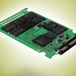
Both the HDD, the core building block of nonvolatile storage in computer systems today, and the SSD are part of a class of storage called block devices. These devices use logical addressing for accessing data and abstracting the physical media using small fixed contiguous segments of bytes as the addressable unit. Each block device consists of three major parts: storage media, a controller for managing the media, and a host interface for accessing the media.
NAND Media
Storage media is the key factor behind the performance and cost advantages of SSDs. Most SSDs are built around widely available NAND flash memory, developed in the late 1980s as an electron-based trapped-charge storage media. The NAND cell stores electrons on a capacitor indefinitely in a no-power state. The charge is then sensed by circuitry on the NAND chip.
Writing to NAND flash is accomplished by either adding electrons (programming) or removing electrons (erasing) to the memory cell using high-voltage pulses. NAND flash is read by using a simple analog-to-digital converter as a bias voltage is applied to the cell.
Different types of flash use different numbers of thresholds to determine the value in a cell. Single-level cell (SLC) stores a single bit of data and has two threshold values. Multilevel cell (MLC) stores two bits of data and has four threshold values. Newer flash memories, called Three-level cell (TLC), are able to store three bits of value with eight or more threshold values. In general the value of an “n” bit A/D convertor can be described as: "n" = log2(#threshold voltages).
A write-verify operation is used to program or erase the NAND flash. A pulse of high voltage is applied to the cell and this process is repeated until the proper value has been programmed into the cell. The big drawback with this technique is that a cell needs to be erased before it can be reprogrammed. Also, the more levels that a flash cell supports, the smaller and more precise the high-voltage pulses must be. Making these pulses more precise slows the programming of the flash and reduces the write performance.
Disk drives use symmetrical access—the minimum read and write accesses are the same size. NAND flash memory, on the other hand, like most nonvolatile memory, uses asymmetrical access—the size of the minimum read and write to the media is dissimilar. This asymmetrical attribute is a result of the architecture of the memory array. Like most memory, NAND consists of a two-dimensional array with a bit line as one dimension of access and a word line as the other dimension of access. The difference in NAND is that multiple cells share the bit line. This NAND string consists of 3264 cells. The smallest size of read is typically an 8KB page, based on the word-line length. A write to the array requires linearly programming all the pages along the NAND string, making the smallest write size 32-64 pages. This is called a program/erase block.
A die is a silicon wafer that consists of one-to-four memory arrays of approximately 4,000 blocks and the elements necessary to make the array usable. These non-storage elements consist of: controller logic for managing operations on the memory array; high-voltage generators necessary for programming and reading from the array; sense detectors for reading the threshold values from the cell; cache buffers for temporarily storing the data bits to and from the memory array; and a high-speed interface for reading and writing data out of the die.
A single die is capable of reading up to 400MB/sec but can write at only 2MB10MB/sec due to the complexity of programming. Latency is a major benefit of NAND flash. Typical latencies are 20200 microseconds for reads and 110 milliseconds for writes. This performance compares favorably with HDDs, where reads and writes are typically measured in tens of milliseconds.
NAND flash dies have a relatively small capacity, holding up to 16GB per die. An SSD contains 8256 dies to meet storage requirements for computing. Because multiple dies will be active at the same time, larger-capacity SSDs tend to yield better performance. Multiple active dies can cause potential thermal problems however, as the high-voltage generators in each die are inefficient. During heavy program and erase operations an SSD limits the number of active dies to avoid overheating or excessive peak current draws.
Electron-based storage has many limitations, as is true of all storage media. The biggest limitations are found in the program and erase operations. The high-voltage pulses will burn out the oxide layer, reducing the cells’ ability to isolate the electrons. Electrons will also become trapped in the oxide layer, adding resistance to the threshold measurement and causing a misread of the threshold value from the cell.
Burnout is the most misunderstood attribute of NAND flash. Manufacturers often specify the number of recommended program and erase cycles per cell for warranty purposes but do not specify the amount of time that a cell will retain data. Even without excessive use, stored electrons will eventually dissipate from the cell, and the data will be lost. The number of program and erase cycles simply accelerates the time before the data fades. Data can be retained for years in lightly cycled cells, while heavily cycled cells may retain data for only a few months. Long exposure to high temperatures also accelerates the decay of data. Numerous reads of the same NAND block can cause electrons to escape, changing the value stored within the cell, which leads to a failure mechanism called read disturbance.
As manufacturing technology improves, allowing the cell size to shrink and reducing the cost, the number of electrons stored per cell shrinks, as does the isolation oxide size per cell. This makes it more difficult to meet the performance and longevity of the previous generation. These limitations, as well as many others, make NAND flash an impractical storage technology by itself. Burnout, data fade, and read disturbance are solvable problems for the SSD, however, as constantly and consistently moving data can prevent such failures. Thus, a symbiotic relationship between NAND flash and the controller is necessary for managing and working around the imperfections on the media.
Controller
The flash controller is the critical component that makes imperfect NAND flash robust and reliable. The controller is a complex embedded system with stand-alone processing and firmware for managing all aspects of the SSD. It is designed to protect and control the underlying NAND flash media.
Similar to a disk drive, the flash controller is most commonly implemented as a system-on-a-chip (SoC) design. The controller consists of multiple hardware-accelerated functional blocks, coupled to one or more embedded processor cores that live within a single application-specific integrated circuit (ASIC) die to provide the cheapest controller cost. Large static RAM (SRAM) for executing the SSD firmware is included in the ASIC, but often external dynamic RAM (DRAM) is used for caching both user data and internal SSD metadata. Higher-end SSDs include a backup power system of batteries or capacitors to ensure the user data in the volatile cache is flushed out to the NAND array during unexpected power loss.
Host Interface
The host interface is the physical interface from the host system to the SSD. The majority of SSDs leverage existing storage standards and interfaces, such as serial ATA (SATA) and serial attached SCSI (SAS). They use traditional block-access protocols. The low-level primitives and high-speed serializer/deserializer are accelerated in hardware, with high-level block-access protocols implemented by firmware running on the embedded processor.
The flash controller is the critical component that makes imperfect NAND flash robust and reliable.
A newer storage interface for SSDs, not used with HDDs, is Peripheral Component Interconnect Express (PCIe). This is the same general-purpose I/O interface used on laptops and servers. This interface is a more efficient interconnect, since it allows systems to phase out the host bus adapter, an additional controller required on SATA and SAS devices to translate these bus protocols. Removing these bus controllers decreases latency and power consumption.
Flash Channel
The flash channel is the controller and interface circuitry dedicated to communication with a physical subset of NAND flash on the SSD. NAND dies are connected to a controller via a parallel I/O interface capable of 400MB/sec of throughput. This interface is shared by four to eight NAND dies, with only one die able to communicate with the flash-channel controller at any one time.
NAND dies with multiple memory arrays are capable of performing multiple operations at once, but they are not fully independent. The die and the channel controller use a lightweight protocol where data is transferred to/from buffers on the NAND die. The controller has to manage and correctly sequence reads, programs, and erase operations to all dies on the channel for the best utilization. Complex array operations, such as program and erase, will render the single memory array or plane busy until the operation is complete. This can take up to tens of milliseconds. Some SSD controllers have dedicated hardware sequencers or microcontrollers with the ability to reorder die operations for optimal performance.
The most common SSD configuration is eight channels, but an SSD controller can have 432 channels to meet performance requirements.
Error Correction
NAND flash has higher performance but also a higher bit error rate than other storage media. The higher error rate requires the SSD to correct bit errors at gigabytes per second, equivalent to the speed of NAND flash. As such, the error-correction hardware responsible for encoding and decoding all reads and writes to the flash is often the largest portion of the SSD controller. Some controllers implement an error-correcting code (ECC) hardware engine for every flash channel to improve parallel performance, while others implement a single ECC engine shared by all the channels to reduce costs.
BCH. The most commonly used ECC is Bose Chaudhuri Hocquenghem (BCH). It is preferred for its speed and ease of implementation, but this comes at the cost of inefficiencies in the redundant storage required for ECC.
NAND flash has higher performance but also a higher bit error rate than other storage media.
Flash-die designers make assumptions on the amount of BCH correctability needed for a given generation of NAND flash and add redundant space within each page and block to account for it. As dies have shrunk with each successive generation of flash, errors and the need for error correction have lifted; the minimum overhead required for correction (rather than storage) has increased five times over the past five years. In addition, controller designs using BCH alone historically assumed that bit failures were uniform. Newer techniques offer more efficiency and correctability based on better understanding of bit failure characteristics and locality of data within the NAND flash die.
LDPC. The use of low-density parity-check (LDPC) code methods along with more advanced information from the NAND die has led to 810 times the correctability over previous BCH methods. LDPC has some drawbacks, however: the correction performance is slower; it requires a significant amount of controller die space to implement; and NAND die designers are often reluctant to share information that would make the LDPC work effectively, as the parametric data needed is often considered a trade secret. A controller might include both BCH and LDPC capability and use LDPC only when the BCH techniques fail, ensuring fast performance with high data reliability.
XOR/Scramblers. Another novel error-correction approach taken from HDD arrays is using XOR parity across a group of NAND dies. This technique should yield better correction with the ability to survive a full NAND die failure. Also, a data scrambler is used to “whiten” the data before it is written to the die. Whitening the data protects against writing certain user data patterns to the NAND die that can cause high bit failures that result from adjacent interference between cells in the memory array.
Controller Firmware
An SSD essentially has a complex file system running internally on the controller. The firmware running this file system is one of the key differentiators among different SSDs today.
Mapping blocks. The primary function of the flash translation layer (FTL) is to map logical blocks from the system to physical NAND pages and blocks. This mapping has the challenge of handling multiple sizes of requests and alignments because of the asymmetrical I/O access limitations of NAND flash. The system uses logical blocks consisting of 512 bytes or 4KB, which then get mapped into 8KB NAND pages, and finally must be written into a block consisting of 64 or 128 pages.
SSDs have no standard technique for overcoming this issue. A common method is statically to map contiguous logical blocks into page-aligned allocation units the size of the NAND page. Once the SSD has enough written allocation units, they are combined into a NAND block-size unit before being written to the flash. Most SSDs today use a derivative of the log-structured file system (LFS) as the basis for the FTL because the append-only write design works well as a result of the erase-before-programming limitation of NAND flash.
Garbage collection. Because writes can be written only to empty blocks, the FTL must maintain a pool of free blocks. If the FTL runs out of free NAND blocks, or if the SSD is inactive for a period of time, the firmware starts performing background garbage-collection operations to reclaim sparsely filled NAND blocks. These NAND blocks are reclaimed by merging the data into new blocks and erasing the old blocks, thus creating a pool of free blocks for use by the FTL.
Early SSDs had performance inconsistency, particularly under excessive stress, because garbage collection either ran out of blocks or used channel/die bandwidth. SSDs today overprovision the physical NAND flash to ensure there are enough free blocks to prevent performance penalties from garbage collection. Most consumer SSDs overprovision less than 5% extra NAND flash, whereas enterprise-class SSDs overprovision up to 50% for performance-critical applications. SSD benchmarks now take into account the impact of garbage collection and require preconditioning the FTL before taking performance measurements.
FTL. The FTL uses a number of methods to optimize performance despite the physical challenges of NAND flash:
- The firmware tracks the number of times each NAND block has been programmed and erased, and it spreads writes evenly across all NAND blocks in the SSD, increasing SSD longevity.
- A certain number of NAND blocks in a die are defective from the die-manufacturing process. Also, blocks can go bad during SSD operation. The FTL must track these bad blocks and substitute good blocks.
- NAND blocks will be marked for garbage collection based on the age of the data in them to avoid data-retention issues.
- The FTL optimizes throughput and die usage. One common method is statically to interleave allocation units across multiple channels to ensure the best possible throughput, as well as the fullest writes of individual blocks.
System Access
Because HDDs have been assumed to be primary storage media, today’s software and hardware are engineered to optimize the performance of these storage devices:
- File systems and applications use complicated heuristics to move the mechanical disk head the minimum distance possible, improving reads and writes.
- Adjacent requests are merged into a single larger request in a process called I/O coalescing, in turn building up the large sequential writes that HDDs handle best.
- There is also an assumption that HDDs will use linear logical addressing where the beginning of the address range is the outside diameter of the disk platter (the fastest part of the drive), and the end of the address range is the inner diameter (the slowest part of the drive).
These techniques, however, do not optimize SSD usage and can hinder SSD performance:
- In an SSD, the logical addressing ends up being completely random, based on the write-access pattern and how the FTL places the data on the NAND flash. This renders locality-based algorithms ineffective.
- Queuing large numbers of I/O requests to SSDs can lead to inconsistencies in latency and performance (both I/O coalescing and the optimization of disk-head placement require substantial queuing of I/O requests).
File systems and applications need to be rewritten to take true advantage of the performance and benefits SSDs can offer. Linux has done the most work optimizing scheduling for SSDs. The operating system has tunables for turning off I/O coalescing and locality-based scheduling heuristics, thus improving the predictability and performance of SSDs.
Some new interface additions for file systems and applications break the HDD emulation model and assist SSD performance:
- TRIM/UNMAP. A common problem with SSDs is that a host file system could erase free data but did not have a way of telling the storage device it no longer needed that data. The TRIM/UNMAP interface lets the SSD clear the logical block addressing (LBA) entries in the FTL, giving it more free space to use in garbage collection and reducing write amplification. OS/X, MS Windows, and Linux have implemented TRIM.
- Scatter Gather. Block-access command protocols limit requests to a single contiguous range of logical blocks, requiring excessive command overhead for small random requests serviced by SSDs. Scatter Gather adds commands for “gathering” multiple noncontiguous requests into a single command, reducing the overhead and improving performance.
While solid-state designs clearly benefit from some of the data-management techniques pioneered in the drive industry, clearly, the HDD emulation model will be broken as we move from the world of computer systems designed for rotating mechanical storage to a world of all solid-state storage.
Solid-State Future
In the future, NAND flash memory will inevitably reach physical limitations. NAND dies are continually shrinking to lower costs, creating endurance and reliability issues that cannot be compensated for by the SSD controller or firmware. Newer memory technologies still in their infancy, such as phase-change memory (PCM) and resistive RAM (ReRAM), show great promise in moving beyond such limitations. They do so in part by shedding the erase-before-programming requirement and the asymmetrical access requirement of the NAND flash used in SSDs.
In turn, this progression invariably will continue the evolutionary/revolutionary paradigm seen today in the transition from rotating media to solid-state devices. These new forms of media will no doubt borrow from, and build upon, the techniques implemented in NAND-based SSDs. At the same time, the shift to these newer technologies will also inevitably require moving beyond the techniques developed today to deal with the unique challenges of NAND. New programming models and interfaces will need to be built to take full advantage of new forms of storage media that offer the speed of DRAM coupled with the data retention of flash.
![]() Related articles
Related articles
on queue.acm.org
Enterprise SSDs
Mark Moshayedi, Patrick Wilkison
http://queue.acm.org/detail.cfm?id=1413263
Flash Disk Opportunity for Server Applications
Jim Gray, Bob Fitzgerald
http://queue.acm.org/detail.cfm?id=1413261
Flash Storage Today
Adam Leventhal
http://queue.acm.org/detail.cfm?id=1413262


Join the Discussion (0)
Become a Member or Sign In to Post a Comment