Real-time image recognition and artificial intelligence (AI) systems require massive amounts of computation, a burden even for today's ultrafast chips, as they consume a lot of energy. Nanophotonics could shift a significant part of this heavy-duty digital number crunching to analog computation, at much greater speed and using almost zero energy.
The basic idea is that reflecting a light wave off a surface with a carefully designed periodic nanostructure changes the wave in a way that represents a basic arithmetical operation. Letting the wave bounce multiple times between the nanostructure and a reflecting layer can be made to represent successive approximations to the solution of a mathematical equation or operation, such as matrix multiplication. This is a basic operation in many kinds of data processing; for instance, by deep learning neural networks.
The Amolf research institute in the Netherlands, working with colleagues at the City University of New York (CUNY) and the University of Pennsylvania, have designed such a metamaterial for analog computation. The researchers published their results in Nature Nanotechnology.
Analog computation using nanophotonics would be particularly relevant for the first stage of data processing, after which conventional digital computing can finish the job. An example that has been studied before is edge detection. Self-driving cars need to analyze their on-board camera images in real time to follow the road and avoid collisions. Edge detection is the first step in identifying objects or persons in these images. Mathematically, this is equivalent to calculating the second derivative of the function that describes the pixel 'landscape' of which a digital image consists.
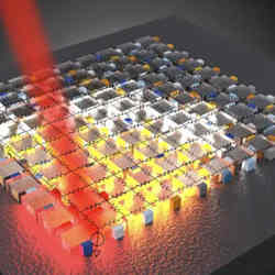
The nanostructure consists of an intricate, tailor-made assembly of silicon islands on a sapphire substrate, which can be produced with the same technology as conventional microchips. The structure is periodic, which means the assembly of islands forms a unit cell that is repeated many times to tile a much larger surface.
On top of that is a partly reflecting, partly transparent layer. The analog computation happens by sending in several plane waves of light that encode the input data. The light bounces up and down between the nanostructured layer at the bottom and the top layer, and the light that finally escapes back through the top layer encodes the output data. It is literally computation at the speed of light, and because it is a passive system, the only energy required is in the input light beams, which is minimal.
The number of reflections determines the accuracy of the answer. It takes about 50 reflections to obtain 64-bit accuracy, the 'double precision' standard for conventional computers. Using this metamaterial, it is indeed possible to read out the signal after that many reflections, says Albert Polman, the researcher who actually made the nanostructure.
The exact shape of a unit cell for a certain calculation is not computable from first principles (i.e. the Maxwell equations for light propagation), so it has to be inverse-engineered. The basic idea is to represent the nanosurface in a computer as an image consisting of a large number of pixels. By specifying a certain simple input, one can determine by trial and error which pixels have to be elevated to produce the desired output. This is the first approximation, which then is subjected to a different input, and the procedure is repeated. Said Andrea Cordaro, first author of the publication in Nature Nanotechnology, "This is basically brute force optimization, which would not be feasible without some clever mathematics to reduce the huge number of possibilities. It is still computationally intensive, but it needs to be done only once."
Polman adds, "We need to check whether the nanostructure that we find is practically feasible. For instance, if the nanostructure has very narrow gaps between elevated 'islands', it cannot be produced with standard chip-technology." Still, the optimization procedure does not produce a unique result, so one can always try again.
Kobus Kuipers, a pioneer in nanophotonics who heads up the QuantumNano department at the Delft University of Technology (although he was not involved in this research), said he is impressed by what was achieved with this metamaterial. "I'm convinced it will become possible to use light for performing certain kinds of computation much faster and with less power consumption. If applied properly, this technology could make the Internet a lot more energy efficient. And the world needs that because the Internet is using ever more electrical power.'
At this stage, these metamaterials are not programmable. The nanostructure represents only one matrix hard-wired into the nanostructure. Polman expects it eventually will be possible to make a metamaterial that can do computations with any matrix, by masking parts of the nanostructure with a task-specific mask. Blocking certain parts of the nanostructure from incoming light would be equivalent to specifying the matrix elements. Such a quickly adaptable mask could be fine-tuned electrically or even mechanically, Polman thinks. Either way, this next phase is still at a very early stage of development.
Compared to matrix computation, edge detection in images is much closer to practical application. In principle, the layer of metamaterial can simply be put in front of the on-board camera of an autonomous vehicle. Says Polman, "Analog edge detection in images has been done before, but it used lenses and optical filters in bulky machinery that could not be miniaturized and built on a chip. Therefore, this field was stalled for 30 years. Now, nanophotonics gets it moving again.'
Arnout Jaspers is a freelance science writer based in Leiden, the Netherlands.


Join the Discussion (0)
Become a Member or Sign In to Post a Comment