As the computing world looks for ways to speed processing and reduce latency across various devices and systems, new and powerful frameworks are emerging. Many of these systems continue to run into the same vexing problem: the interconnects on microchips use electronic signals to transport data over copper wire between integrated circuits (IC).
"Copper is a dependable but somewhat inefficient technology. Interference and signal degradation occurs when high speed electrical signals are carried over closely spaced metal traces," according to Keren Bergman, Charles Batchelor Professor of Electrical Engineering at Columbia University. As a result, researchers are exploring ways to introduce on-chip electro-optical interconnects that push performance far beyond today's 100s of gigabits per second (Gbps) chip edge bandwidths and into the realm of 100 Terabits per second (Tbps) or faster, all while dramatically reducing energy consumption.
Optical interconnects are not a new idea. The notion of using photons and light on chips has been around for a couple of decades, and fiber optic technology already is used widely for telecommunications, computer cabling, and transceivers in datacenters. It also serves as the backbone for the Internet. Yet packing the technology into semiconductors represents a significant challenge that spans laser systems, chips design, packaging, and fabrication methods.
Lighting a Pathway
At the center of the quest to develop faster and more energy-efficient chip-level interconnects is Moore's law. Today's systems increasingly butt up the physical limits of the framework, which says that the number of transistors used in a dense integrated circuit doubles approximately every two years.
"Today, performance isn't limited so much by raw compute power but our ability to move data from one place to another," says Gordon Keeler, program manager in the Microsystems Technology Office of the U.S. Defense Department's Defense Advanced Research Projects (DARPA). Adds Ian Karlin, principle HPC strategist at the U.S. Department of Energy's Lawrence Livermore National Laboratory, "We are seeing ever diminishing returns."
While several innovative chip designs are on the horizon, including RISC-V, neuromorphic semiconductors, and nanosheet transistors, all are currently beholden to electrical (copper) interconnects. "Optical interconnects remove the interference and data loss that occurs over copper. It provides a tremendous amount of bandwidth," Bergman explains. "You can propagate signals over relatively long distances before you have to re-amplify them."
In practical terms, this means that a wide range of current devices, including smartphones, personal computers, Internet of Things (IoT) devices, autonomous machines, and high-performance computing clusters would operate far more efficiently. It opens up wider system design options, such as coupling deep learning accelerators over the network into HPC systems. "It's a game changer," Karlin says. "It could have a huge impact on HPC plus AI workloads."
The technology also offers a high level of flexibility in chip design and usage models. With modular chiplets, semiconductor manufacturers could design microprocessors with optical interconnects for highly specialized tasks such as optical spectroscopy, gas sensing, LiDAR, portable atomic clocks, high-bandwidth secure communications, and intrusion detection, among other areas. Optical interconnects are particularly suited to situations where "you're moving enormous amounts of data…or there's a need for low latency," Keeler explains.
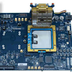
The concept took a giant step forward in May 2020, when DARPA's Photonics in the Package for Extreme Scalability (PIPES) program, which includes Ayar Labs and Intel, announced a breakthrough that substantially improved interconnect reach, efficiency, and latency. Using an Ayar Labs optical interface called TeraPHY, an optical I/O chiplet that replaces electrical serializer/deserializer (SERDES) chiplets, and Intel's advanced packaging and interconnect technology, researchers demonstrated the capability for 2 Terabits per second (Tbps) of bandwidth.
Says Hugo Saleh, vice president of marketing and business development at Ayar Labs, "The technology is advancing rapidly. We're at the point where it's possible to deliver a 1000x improvement in interconnect bandwidth density at 10x lower power."
Better Connections
There is no question that optical interconnects will significantly improve computing speed and reduce energy consumption, yet a few hurdles remain. One of the biggest, Bergman says, revolves around chip packaging. "At present, there are no standards and many different approaches for designs, including the use of lasers."
Another is basic economics. "It's still a pretty nascent world in terms of scale and maturity. Large manufacturers aren't going to commit to fabricating high volumes until the demand exists," she notes.
Perfecting optical components will require more research. Interconnect technology ultimately could incorporate dense wavelength-division multiplexing, which relies on multicolor lasers, or a single laser that can generate a comb of frequencies. In some cases, a combination of laser technology may be required for different devices, systems, and scenarios. "The development of a more capable integrated platform tailored to specialty user needs could have revolutionary impact," Keeler says.
Concludes Saleh, "We have reached a point where computing systems are severely constrained by the interconnects. Future systems will be impacted further by bandwidth limitations. Optical interconnect technology maximizes the performance of computing systems."
Samuel Greengard is an author and journalist based in West Linn, OR, USA.


Join the Discussion (0)
Become a Member or Sign In to Post a Comment