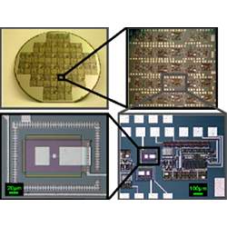
Most micro-electro-mechanical systems (MEMS) inside your smartphone, smartwatch, or other wearable electronic device require a pair of silicon dice—one die for the MEMS moving parts, and one die for its complementary metal oxide semiconductor (CMOS) supporting electronics—requiring at least four cubic millimeters.
U.K.-based nanodevice startup Nanusens has developed a MEMS-inside-CMOS process, which yields a device that fits on a single cubic-millimeter chip-scale package (the same size as a chip's die).
Said Mike Feibus, principal analyst at Scottsdale, AZ market intelligence firm FeibusTech, "Embedding MEMS components right into CMOS will result in products that are far smaller, cheaper and lower power than conventional MEMS."
Manuel Tagliavini, principal analyst of MEMS at information provider IHS Markit, said Nanusens "is working with several Bluetooth earbud suppliers, which will use their chips to add smart wake-up, tap, and double-tap functions to their reference designs." Tagliavini said the small dimensions of earbuds "not only reduces their power usage, but also reduces the stiction problem that affects traditional MEMS sensors. And their very thin package—as thin as 0.4 millimeters—fits nicely inside really small wearables like earbuds."
In the physics community, the nanscopic scale ranges from 1 to 100 nanometers (billionths of a meter), but in the MEMS community, the nanoscale is from 1 to 100 microns (millionths of a meter)—equivalent to the mesoscopic scale in physics. At 100 microns and smaller, Nanusens devices qualify for the label nano-electro-mechanical systems (NEMS)—smaller than MEMS, but larger than individual molecules. Consequently, Nanosens' NEMS devices open the door to custom multifunctional chips that can hold all a smartphone's or wearable's MEMS functions—as stacked NEMS devices—within a single cubic millimeter of CMOS.
NEMS-inside-CMOS makes use of a six-metallization-layer process ordinarily used for interconnecting the transistors at the top of a CMOS chip. Burying the metal moving parts of the NEMS device in a sea of silicon dioxide enables Nanusens to chemically etch away the silicon dioxide, freeing the metal moving parts to perform their functions inside the single chip. CMOS chips alone have no moving parts—only electronics—but by burying moving parts inside an otherwise-solid CMOS die, a much smaller and less expensive single-die chip can perform both functions.
"Almost every other MEMS device has to be fabricated in two facilities; one for the moving parts and one for the electronics. They are usually combined inside a microchip's package using wire bonding to connect them," said Nanusens CEO Josep Montanyà, "but we require only a single CMOS die, which can contain inside itself up to six different MEMS devices."
The most popular MEMS functions today include accelerometers (which automatically rotate device displays from landscape to portrait mode), gyroscopes (which detect your device's movements in three-dimensional space), motion detection (which automatically turns your device "on" when you pick it up), radio-frequency switches (that adapt your device's antenna to changing environmental conditions), and microphones so small that multiple units can form beams to follow your speech as it moves relative to your device, while cancelling background noise.
The most advanced MEMS manufacturers today take the MEMS wafer with thousands of dice on it, and the CMOS wafer with the same layout of electronic dice, and bond them together face to face before dicing them into two-layered MEMOS-on-CMOS chips, eliminating the need to wire-bond the two dice side by side in a large chip package. Nanosens says its versions of popular MEMS devices will only a single wafer and no bonding step, and will greatly reduce the size of mechanical parts to under 100 microns.
"Freeing up space inside smaller wearables, such as earbuds, will also extend their battery life in two ways; by using less current because of the nanoscale size of our single chip, plus saving space so that bigger batteries can be fit inside the ear bud," said Montanyà.
At Mobile World Congress 2019 in Barcelona, Spain, in February, Nanusens demonstrated RF MEMS chips engineered to tune antennas to the frequencies required by smartphones, as well as performing impedance matching. San Jose-based Cavendish Kinetics already makes chips that perform this function; Nanusens claims its process is less expensive.
Also at Mobile World Congress, Nanusens demonstrated its first motion detector, a device can turn on an idle smartphone in which it is installed when it are picked up, as well as detecting taps and double-taps. These functions are performed by accelerometers today, but Nanusens claims its lower-bandwidth motion detector does the same job while consuming less power.
Later this year, Nanusens plans to release its first bone conduction sensor, which processes vibrations from the voice in the bones of the inner ear, working together with an actuator that vibrates the bones of the inner ear, both bypassing the ear canal.
Next year, the company plans to introduce multiple NEMS-in-CMOS devices in a single package, which will save printed circuit board (PCB) space, enabling smaller wearables such as wireless Bluetooth earbuds to utilize larger batteries that take advantage of the extra cubic millimeters of space. The lower power requirements of multi-sensor NEMS, plus the extra space for larger batteries, could extend battery life up to 20% for small wearables, according to Nanusens.
A study and forecast of the market for nanoelectromechanical systems by Variant Market Research identifies key players in the market for NEMS as including Agilent Technologies, Bruker Corporation, Showa Denko K.K., Analog Devices, Inc., Materials And Electrochemical Research Corporation, Vistec Electron Beam GmbH, Graphene Frontiers, Amprius, Inc., Broadcom Corporation, and Inframat Corporation.
R. Colin Johnson is a Kyoto Prize Fellow who has worked as a technology journalist for two decades.


Join the Discussion (0)
Become a Member or Sign In to Post a Comment