More than 20 years ago, the historical rate of shrinking transistors to improve speed, density, power consumption, and cost became impossible to maintain. Even with slower physical scaling, however, electronics manufacturers steadily improved their products by exploiting new materials, new device and circuit designs, and faster communication between chips.
Many researchers believe there is a new opportunity to dramatically improve the transistors themselves by fashioning them out of the atomically thin sheets that naturally form in graphene and related layered materials. Incorporating a new material into highly optimized, state-of-the-art manufacturing will not be easy, although industry has done it before. It may start by grafting two-dimensional (2D) materials onto traditional chips to provide special capabilities, such as better interconnections or integrated optical devices. “Some form of 2D materials is going to be introduced integrally into the electronics eventually,” said Xiangfeng Duan of the University of California, Los Angeles (UCLA).
Graphene Dreams
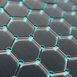
Graphene—carbon atoms arranged in a chicken-wire-like sheet—has been the archetypical 2D material since the mid-2000s, when U.K.-based physicists realized they could peel single graphene layers off a chunk of graphite using adhesive tape. (They received the Nobel Prize for their work in 2010.)
Graphene and several other 2D materials feature strong covalent bonds between atoms within the layers, which are in turn stuck together only weakly. This makes it easy to reproducibly create sheets of material that may be centimeters across but only one or a few atoms in thickness, which are ideal for making short, fast field-effect transistors (FETs).
Moreover, because no bonds need be broken, the exposed surfaces are highly perfect, with few defects that disrupt electron motion within the layers. Electrons in graphene have a much higher mobility than they do in common semiconductors, which also translates into very fast transistors. Physicists continue to find exotic new effects in graphene, such as superconductivity that arises when two graphene sheets are slightly rotated relative to each other.
Graphene, however, has a fatal flaw, at least for large digital circuits: it is not a semiconductor. It is a semimetal, meaning that its conductivity never gets very small. Turning almost all of the billions of transistors in a chip completely off—with currents orders of magnitude smaller than when they are on—is essential to limit its power consumption.
Over the years, researchers have proposed various ways to transform graphene into a true semiconductor, such as preparing it as narrow nanoribbons. Manufacturing chips from such tiny filaments is hard, as it has proved for their cousins, carbon nanotubes.
“There’s lots of progress, but it’s an extraordinary challenge when you think about from the scaled integration point of view,” Duan said. “If you want six-nines yields [99.9999%], then it becomes very difficult to assemble these nanoscale-dimension materials, either nanoribbons or nanotubes.”
Still, academic researchers keep exploring new ways to manipulate graphene. Recently, Manoj Tripathi of the University of Sussex in the U.K. and his colleagues showed that tiny folds in a graphene sheet can change the local electronic structure, similarly to the doping changes that are used in traditional bipolar transistors. “We found that a single wrinkle is able to make a transistor,” Tripathi said, although he acknowledged it would be a long road to making useful circuits out of these tiny devices.
Beyond Digital Logic
“At the beginning, it was thought that graphene could be used in logic, but it’s not true. It’s a semimetal, so it’s always on,” said Amaia Zurutuza, chief scientific officer of Graphenea, a graphene supplier in San Sebastián, Spain.
Still, graphene sheets are already being used in other products.
“Most of the applications that we are pursuing (not directly, but in collaboration with customers) are combining graphene with silicon,” she said. For example, the Finnish company Emberion offers infrared and thermal imagers that use the semiconductor-like properties of graphene for light detection, placing the layers on top of traditional silicon integrated circuits. The surface sensitivity of a thin graphene layer can also be exploited for detecting molecules, as well as light.
Graphene also could be useful for replacing or augmenting the wiring that connects transistors in a circuit, which also are formed after the devices are finished.
In the longer term, Zurutuza said, companies are exploring the possibility of coupling thin graphene devices with silicon photonics for telecommunications. “Sensors are considered lower-hanging fruit, because this requires back-end-of-the-line integration [after the sensitive and high-temperature processes that make the transistors], so the requirements for integration are not as stringent,” said Deji Akinwande of the University of Texas at Austin. Similarly, graphene-based memory might be stacked on chips late in the process.
Graphene could also be useful for replacing or augmenting the wiring that connects transistors in a circuit, which also are formed after the devices are finished. Ever-denser chips require ever-smaller wires, and often “graphene is more robust than copper,” Akinwande said. “It’s more reliable. It can handle more current. For a lot of the metrics that you care about for interconnects, the graphene-based material outperforms the existing copper, especially for scaled nodes.”
Beyond Graphene
“Scaled nodes” refers to the regular succession of integrated circuit technology generations, as prescribed by Moore’s law. In the early decades, these generations were named after the shortest gate electrode of FETs, with other dimensions shrinking proportionally. That label lost its meaning around the turn of the century, however. “The whole idea of scaling is now some kind of ambiguous idea,” Akinwande said. “It becomes unclear whether this is just a marketing term.”
Unfortunately for researchers, since 2015 the semiconductor industry no longer publishes detailed specifications for future transistors. The revised document, the International Roadmap for Devices and Systems, “is more of a systems-level roadmap, so it doesn’t provide a lot of details for devices,” Akinwande said. “It’s kind of a free-for-all, at least in academia, how to push the boundary forward.”
Leading semiconductor manufacturers continued to drive dramatic progress in density and performance, but gate length stopped keeping pace with the label. One reason for this was the difficulty of shrinking the vertical dimensions of the transistor as it gets shorter, which allows the gate electrode to electrostatically control the channel to turn its conductivity on and off. Cutting-edge integrated circuits instead achieve this control using the FinFET device design.
Semimetallic graphene cannot exploit the improved control of short-channel effects in spite of its thinness, but there are numerous other layered materials that are intrinsically semiconducting. The most studied materials are the transition-metal dichalcogenides, abbreviated as TMDs or TMDCs, including molybdenum disulfide (MoS2), tungsten diselenide (WSe2), and indium diselenide (InSe2) and many other materials. (Transition metals comprise the dozens of elements in the center of the periodic table, while chalcogens are the group VI elements sulfur, selenium, and tellurium.).
“Even five years ago, hardly any semiconductor industry company was investing in this, but now you see internal R&D is now emerging for trying to integrate these TMDs for scaled nodes,” said Akinwande. “They have very good transistor performance.” In contrast, he said, “As you make silicon thinner and thinner to make smaller transistors, the mobility falls of a cliff.”
A New Manufacturing Ecosystem
One important consideration in material choice, in addition to device performance, process complexity, and thermal stability, is toxicity, said Cedric Huyghebaert, program manager for exploratory materials and modules at the Interuniversity Microelectronics Centre (IMEC) in Belgium. As the technical leader of a new European project called 2D-EPL (Experimental Pilot Line), he noted that selenide processing uses very toxic chemicals. Because of the resulting environmental health and safety challenges if they were to be used on an industrial scale, the project is currently focusing on the sulfides MoS2 and WS2, in addition to graphene.

Figure. “Islands” of gold atoms deposited on a layer of two-dimensional molybdenum sulfide, produced by Massachusetts Institute of Technology researchers using a new scanning transmission electron microscope.
In most current explorations of 2D materials, “Typically they are grown on a template or on a catalyst metal, and then they are transferred” to the final wafer, Huyghebaert said. Because this process includes manual steps, “It brings a lot of variability, and this is not according to semiconductor standards.”
“The 2D-EPL project is to try to set up an ecosystem” Huyghebaert said, to support and automate these processes, including materials suppliers, tool manufacturers, and device makers. “The product is only possible when you have the whole ecosystem.”
By contrast, semiconductor manufacturers historically deposit materials as molecules onto partially processed wafers. “If you can grow directly these 2D materials onto an amorphous dielectric with the right quality, this will be the preferred option,” Huyghebaert acknowledged, but so far it has not been possible to get 2D materials of sufficiently high quality in this way, especially for graphene.
Moreover, he said, “The other reason why transferring could be quite interesting is that it would allow you to do heterostacking of these 2D materials,” combining layers of different materials using techniques like those that have recently been developed to vertically package silicon devices. “Transferring very thin layers … would be very powerful in the longer term for the semiconductor industry and nanotechnology.”
For ultra-short transistors, Huyghebaert said, “The very appealing thing about TMDCs is that it would reopen the door for classical scaling for two to three generations.” Still, he said, even if scaling is not successful, “There will be so many other opportunities that it will pay off in any case.”
 Further Reading
Akinwande, D., Huyghebaert, C., Wang, CH., et al.
Graphene and two-dimensional materials for silicon technology. Nature 573, 507–518 (2019). https://doi.org/10.1038/s41586-019-1573-9
Liu, Y., Duan, X., Shin, H.J., et al.
Promises and prospects of two-dimensional transistors. Nature 591, 43–53 (2021). https://doi.org/10.1038/s41586-021-03339-z


Join the Discussion (0)
Become a Member or Sign In to Post a Comment