For decades, computers have grown more powerful because chipmakers have been able to make ever-smaller transistors, allowing them to cram more onto a single chip. That steady march has always depended on optics—shorter wavelengths of light allowed chipmakers to draw smaller lines for circuit paths, which then can be closer together. It has become increasingly harder, however, to reach the high resolutions needed for ever-tinier features.
The answer, or at least part of it, may lie not with optics at all, but with chemistry. Researchers in both industry and academia are trying to perfect a process that would let chemicals arrange themselves into tiny lines to serve as a pattern for the circuits. The lines and spaces in most chips now are on the order of 40 nanometers (nm) wide, but are expected to drop to less than 10 nm within a few years.
“Ten nanometers is really where they’re going to be forced to implement some new technology,” says Christopher Ober, professor of materials engineering at Cornell University in Ithaca, NY. The technology Ober and others are interested in is directed self-assembly (DSA), in which materials called block copolymers arrange themselves into a desired pattern.
Block copolymers consist of two different materials that do not like to mix, like oil and water, but they are bonded together, so they cannot fully separate. When liquid block copolymers are heated, they form a structure in which each polymer has the least possible contact with the other. They might, for instance, form alternating stripes of each polymer, or create a checkerboard pattern, depending on how they were designed.
In chip manufacturing, that would mean coating the silicon wafer with a neutral chemical to act as a base, then adding the block copolymer on top, and heating the whole thing. The polymers would form alternating lines—think of them as red stripes and blue stripes—and one set, say the red, would be washed away. The remaining blue stripes would act as a pattern for the same etching process used in current photolithography to inscribe circuits into silicon.

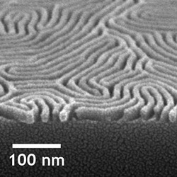
Figure. Self-assembly of block copolymers on a flat substrate normally create fingerprint-like patterns having nanodomains with no long-range order (left). To fabricate well-aligned nanostructures over a large area, the self-assembly of the block copolymers can be induced in a confined space on the sub-micrometer scale.
Photolithography also relies on chemicals—photoresists that are patterned through exposure to light, creating a pattern that is used to define which parts of the wafer to etch. Many modern designs, however, require multiple masks, driving up costs. The machines for focusing the light beams to ever-smaller sizes are also expensive, so DSA could, the thinking goes, create smaller features and do it more cheaply.
A few years ago, DSA was seen as the next big thing, and many chipmakers were investing heavily in it, says Kurt Ronse, director of the advanced lithography research program at the Inter-university Microelectronics Center (imec) in Leuven, Belgium. The focus was on a block copolymer consisting of polystyrene and polymethyl methacrylate, or PS-PMMA, which was targeted for features with a 28nm pitch, in which lines and spaces are each 14nm wide. At the time, the anticipated next photolithography technology was extreme ultraviolet (EUV), but progress toward making it commercial seemed to be stalled.
Too Many Defects
The hype over DSA did not last, says Ronse. “Very quickly it turned out that one of the big issues was going to be defects,” he says. Sometimes the copolymer would leave a gap, or the stripes would get too close to each other or even cross, a phenomenon called “line edge roughness.” The undercoating might have a pinhole or a slight bump that would throw the process off.
“It uses thermodynamics to form the patterns,” says Charles Black, director of the Center for Functional Nanomaterials at Brookhaven National Laboratory in Upton, NY. “It usually ends up with a defect here or a defect there, and microelectronics is really intolerant of that.”
Over time, Ronse says, researchers managed to reduce the level of defects, while at the same time, EUV was beginning to look more promising. The combination made it seem less likely that DSA would provide the low-cost alternative the industry sought. “After a couple of years of development, the window of opportunity for 28nm pitch was starting to close,” Ronse says.
Because self-assembly is a thermodynamic process, it is controlled by differences in surface energy, and the top “surface” is open air.
Though the hype has faded, he says, work continues. Some of the companies imec works with have ended their DSA research, while others are still going, though they have directed some of their chemistry work toward developing photoresists for EUV. “They have not stopped DSA development, but by putting less effort in it, it definitely slows down,” Ronse says.
While research into DSA is not as aggressive as it once was, it has not stopped, says Christopher Ellison, associate professor of chemical engineering at the University of Minnesota. “I don’t think it’s going away,” he says. “It’s not growing at a rapid rate.”
Part of the reason for that slowdown may be that it is not the optical physics that the chipmaking industry has always relied upon. “It makes it challenging for industry to accept because it’s so radically different,” Ellison says.
Surface Tension
While PS-PMMA may seem less attractive than it once did because its resolution limit is 11 nm, chemists are pursuing other block copolymers that could go even smaller. Some materials have a high chi, a measure of how incompatible the two polymers are. High-chi copolymers can perform the same self-assembly as PS-PMMA, but at a smaller size. Ellison’s group has created structures just four to five nm wide.
The trouble with high-chi copolymers is that it can be difficult to get them to stand up straight. To form parallel strips, they need to orient themselves perpendicular to the surface they are on. Often, however, they will flop over onto their sides, destroying the pattern.
Because self-assembly is a thermodynamic process, it is controlled by differences in surface energy, and the top “surface” is open air. Some researchers, such as Ellison and his colleague C. Grant Willson, a professor of chemical engineering at the University of Texas at Austin, have been working on topcoats, films of chemicals that change the surface energy on top of the copolymer so that it aligns itself correctly.
Paul Nealey, a professor of molecular engineering at the University of Chicago and one of the pioneers of DSA, says there are three or four methods to control the orientation of high-chi materials. Nealey and Karen Gleason, a professor of chemical engineering at the Massachusetts Institute of Technology, Cambridge, MA, published a paper in Nature Nanotechnology in March in which they reported using a technique called initiated chemical vapor deposition to create a topcoat that forced the block copolymer to line up the way they wanted it. The approach allowed them to create features only 9.3nm wide.
Another approach exposes the copolymer to vapor from a solvent to change the balance of energy. A technique explored by IBM mixes in an additive to the copolymer that changes how it responds to surface energy at the air interface.
However they are controlled, block copolymers cannot do everything on their own. Some lithography must be used to inscribe guiding lines for them to follow—that is the “directed” part of DSA. Because the material forms lines much thinner than those inscribed, they require less-advanced photolithography processes. At some resolutions, the guiding pattern could be created by the current state-of-the-art process, 193nm immersion lithography, which uses a liquid to focus the light beam to a smaller area. It could appeal to industry to use DSA with immersion lithography equipment that is already paid for, rather than needing to invest in new equipment for EUV. The extra expense of DSA is minimal, Ober says; “It’s just an extra bottle of photoresist.”
In fact, EUV and DSA may turn out to be complementary technologies, each doing things that are difficult for the other. The first use for DSA, the researchers say, will not be for drawing lines at all, but for controlling the size of the holes through which different layers of transistors are connected. Conventional lithography makes those holes, or vias, too large. They could be filled with a block copolymer, which would assemble to form a narrower channel through which connections could be made.
Design Challenges
One shortcoming of DSA is that it cannot inscribe sharp 90-degree turns, while photolithography can. Any of these technologies will impose some constraints on chip designers, but chip architects have learned to deal with the existing ones, Ober says. “You have a set of shapes and forms you can produce,” he says. “People have got very clever at taking these limited set of shapes and learning how to arrange them.”
Researchers will continue to push ahead with DSA, Ronse says, seeking the right blend of polymers, working on ways to keep the chemicals consistent from one batch to the next, and finding ways to bring down the number of defects to acceptable levels.
At the same time, the industry will push forward with EUV. The technology has failed to materialize despite a couple decades of development, but it may have turned a corner; “Although it looked like it was never going to happen, now it looks really, really close,” Ober says.
While it is not certain what mix of technologies will succeed, the researchers are not worried about reaching the limits of semiconductor technology any time soon. “The demise of photolithography has been predicted forever,” Black says. “Probably for 20 years people have been saying ‘the end is here,’ and those photolithography guys have been coming up with ways to get around it.”
 Further Reading
Self-Assembly: Lego Blocks in Nature Paul Nealey, University of Chicago https://vimeo.com/138700499
Suh, H.S., Kim, D.H., Moni, P., Xiong, S., Ocola, L.E., Zaluzec, N., Gleason, K., and Nealey, P.F.
Sub-10-nm patterning via directed self-assembly of block copolymer films with a vapour-phase deposited topcoat, Nature Nanotechnology 12, 2017 http://www.nature.com/nnano/journal/v12/n6/full/nnano.2017.34.html
Sinturel, C., Bates, F.S., and Hillmyer, M.A.
High X-Low N Block Polymers: How Far Can We Go?, ACS Macro Letters 4, 2015
Jiang, J., Jacobs, A., Thompson, M. O., and Ober, C. K.
Laser spike annealing of DSA photoresists, J Photopolymer Science and Technology 28, 2015. https://www.jstage.jst.go.jp/article/photopolymer/28/5/28_631/_article
Lane, A.P., Maher, M.J., Willson, C.G., and Ellison, C.J.
Photopatterning of Block Copolymer Thin Films, ACS Macro Letters 5, 2016 http://pubs.acs.org/doi/abs/10.1021/acsmacrolett.6b00075


Join the Discussion (0)
Become a Member or Sign In to Post a Comment