The end is not near for integrated circuits based on the predictions of Moore’s Law, according to Intel, IBM, Micron Technology, Qualcomm, Raytheon, Texas Instruments, and others who are collaborating on one of two efforts (or both) at the U.S. non-profit research consortium Semiconductor Research Corp. (SRC) called the Nanoelectronics Research Initiative (NRI) and StarNet.
For instance, Intel revealed at the recent ACM Special Interest Group on Design Automation (SIGDA) International Symposium on Physical Design (ISPD 2017) that it is working on over a dozen alternatives to complementary metal oxide semiconductors (CMOS), many inspired by NRI and StarNet, to extend Moore’s Law indefinitely.
Semiconductor foundries Global Foundries and the Taiwan Semiconductor Manufacturing Corp. are working with SRC to adapt existing CMOS foundries to be compatible with new technologies aimed at keeping Moore’s Law going.
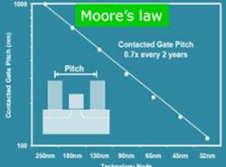
Moore’s Law is rooted in a 1968 paper by Intel co-founder Gordon Moore, and modified by remarks he made in 1975, forecasting that semiconductor performance/complexity would double every year until about 1980; after that, it would double every two years. In the past, that doubling of capacity/performance was obtained by shrinking the design of chips to double the number of transistors in the same form-factor, thus doubling performance (or, using the same number of transistors on a chip half the size, thus halving its cost).
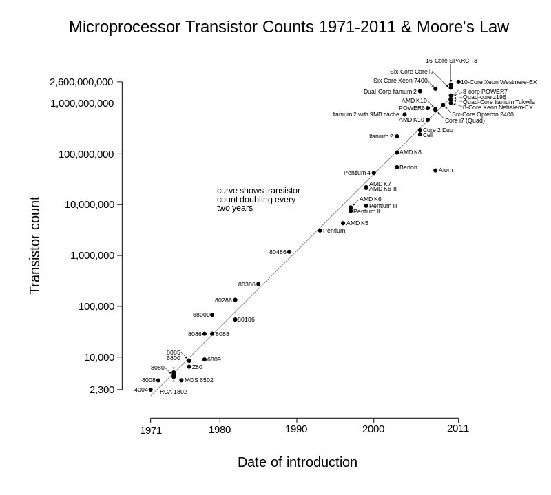
Transistor counts for integrated circuits plotted against their dates of introduction.
The curve shows the doubling of transistor counts every two years.
Credit: Wgsimon
Current chip technology using 20-nanometer design rules will hit a brick wall after three more size-reductions to the 5-nanometer node, according to the International Technology Roadmap for Semiconductors, which has tracked Moore’s Law chip scaling since 1992. Intel, and other firms, are intent on keeping this from happening.
“We intend to augment CMOS, which will still be used for I/O [input/output] and other functions that require analog circuits,” said Intel Senior Fellow Ian Young. “Our new technologies will need to pass all the same tenets of logic as CMOS; namely, exhibit nonlinear characteristics, provide power gain for fan-out, support concatenation, prevent feedback, and provide the complete set of Boolean operations.”
Those requirements, which focus on spintronics and magnetoelectronics, were agreed upon by IBM, Texas Instruments, and Micron for NRI, plus Raytheon and Qualcomm for STARNet, according to SRC chief executive officer Ken Hansen. “SRC’s model is for its members to define a ‘need’ document which they come up with among themselves, then SRC contracts universities eager to fulfill those needs with all participating members having free access to the resulting intellectual property (IP) of the proposed solutions.”
Said NRI executive director An Chen, “future generations of electronics will be based on new devices and circuit architectures, operating on physical principles that cannot be exploited by conventional transistors. NRI seeks the next device that will propel computing beyond the limitations of current technology.”
Contributing to both programs is the Semiconductor Industry Association (SIA), which in March released the white paper Semiconductor Research Opportunities: An Industry Vision and Guide jointly written by Intel, IBM, Texas Instruments, Micron, TSMC, Qualcomm, Analog Devices, Applied Materials, and 62 other contributors. “A new roadmap of technology beyond silicon is required…such as low-power, low-voltage, beyond-CMOS logic and memory devices,” according to the white paper. “The requirements for novel devices have to factor in advances in and requirements for alternative architectures such as neuromorphic architectures.”
On the government side, the U.S. National Institute of Standards and Technology (NIST), the National Science Foundation (NSF), the State of Nebraska, the State of New York, and the State of Texas have helped to fund NRI; the Defense Advanced Research Projects Agency (DARPA) and the U.S. Air Force Research Laboratory have helped to fund STARnet.
“NRI and STARnet are both looking to extend Moore’s Law,” said Hansen. “Our architected approaches address how we can extend Moore’s Law without scaling by uncovering how can we exploit new device types with different architectures to provide more performance at lower cost.”
Hansen said both NRI and STARnet were in their last year, to be supplanted in 2018 by SRC’s Joint University Microelectronics Program (JUMP) and the Nanoelectronic COmputing REsearch (Ncore) program, which will directly address how to drive Moore’s Law further using not only inorganic materials, but also using what he called “bio-electronic solutions” that mimic the low-power operation of the brain (which consumes just 20 watts of electricity to outperform supercomputers that require megawatts). Hansen said power consumption “is the biggest challenge we have in the semiconductor industry.”
Spintronics—using electrical dipoles, magnetic dipoles, or the orbital state of atoms to represent the 1s and 0s of binary code—was the primary focus at NRI and STARnet efforts to reduce the size, and speed up the encoding mechanism, for existing chips. Today, charge encodes ones and zeros using over 10,000 electrons per bit; spintronics could halve the number of electrons required to do so every two years, thus extending Moore’s Law at least another 20 years. The Ramtron unit of Cypress Semiconductor already is using magnetic spin transfer torque to not only lower power consumption of memory chips, but also to simultaneously speed up the time it takes to change a bit from 1 to 0—or visa versa—to 10 femtoseconds, compared to 300 picoseconds (300,000 times longer) for CMOS.
NRI’s Chen identified “low-voltage and low-power devices based on novel switching mechanisms or even alternative state variables beyond charge” as “important research directions in both programs.
“Spintronic and magneto-electric devices may potentially lower switching voltage, reduce power dissipation, and enable memory functions. Spin-based MRAM (magnetic random-access memory) and STTRAM are very promising memory technologies. Spintronics for logic applications is more challenging, but represents an compelling opportunity for research.”
R. Colin Johnson is a Kyoto Prize Fellow who has worked as a technology journalist for two decades.


Join the Discussion (0)
Become a Member or Sign In to Post a Comment