Over the last decade or so, there have been a number of efforts to stack chips into so-called "towers" to boost overall system performance and meet the needs of power-hungry applications, but few of them panned out significantly. Now, a team at Stanford University has presented a model of a monolithic 3D stack that incorporates logic and memory together and which, they say, can be mass-produced.
Three-dimensional (3D) chips today are typically made with chip-stacking, which is when the different vertical layers are built on separate substrates, and then physically stacked and bonded one on top of the other, explains team member Max Shulaker, a Stanford graduate student. The different vertical layers are then connected with vias (electrical connections between layers of a circuit) called Through-Silicon Vias (TSVs), which are very large and cannot be packed densely.
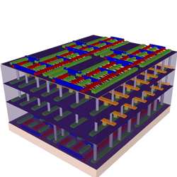
Monolithic 3D, as demonstrated by the Stanford team, allows each layer of the circuit to be built directly over the previously fabricated layers, all on the same starting substrate, Shulaker says. Because of this monolithic 3D integration, nano-sized vias more than 1,000 times denser than TSVs can be used to connect the vertical circuit layers, he says, allowing for a massive increase in vertical connectivity between circuit layers.
"That’s important because if we build logic and memory on two different layers, we can have a massive amount of connectivity between layers,’’ says Shulaker. "That translates to both the logic and memory being physically closer together because the wires are shorter and the interconnections are more numerous. [That creates] an increase in logic and memory bandwidth, which means we can move a lot more data back and forth."
The new high-rise chip architecture was detailed in a paper the Stanford team presented at the IEEE Electron Devices Meeting last December. The work was led by Subhasish Mitra, a Stanford associate professor of electrical engineering and computer science, and H.S. Philip Wong, a professor of electrical engineering in Stanford’s School of Engineering.
Chips traditionally have been developed using silicon transistors, but that creates a challenge when monolithically stacking them because that creates very high temperatures. "To build a transistor today takes more than 1,000 degrees Celsius,’’ notes Shulaker. "The problem is, by the time you build your upper circuit layers, the temperature will damage or destroy the bottom layer circuits and all the metal wires connecting them." Some electricity also leaks out of silicon transistors, even when they are shut off, he says.
The Stanford group’s goal was to come up with energy efficient transistors, which required new materials. That led them to use carbon nanotube (CNT) transistors, which Shulaker says can be assembled with temperatures below 200 degrees Celsius. CNTs also provide greater speed while using less energy, he says.
The team is also using new memory technologies known as resistive random access memory (RRAM) and spin-transfer torque, which result in energy-efficient, dense, non-volatile memories, which Shulaker says can also be built at very low temperatures. As a result, he says, "Not only do we get the benefit of using new devices, but we can also build new system architectures like monolithic 3D." The Stanford model uses four layers of logic on top of memory.
Additionally, monolithic 3D integration of logic and memory can allow for new architectures and potentially alleviate logic-memory communication bottlenecks, industry observers say.
The Stanford approach is interesting because of the vertical integration of resistive memory and carbon nanotubes with silicon, notes David Kanter, an analyst with The Linley Group. Resistive memory is a very niche product and carbon nanotubes have only been used so far for research purposes, he says.
"The focus on low-temperature steps and heterogeneous integration and using interlayer vias is not something people are putting into production today,’’ Kanter says. "The question is not how will this change the world … but when will we see companies in the industry looking at this and starting to adopting similar techniques in their research? Once you see Intel or IBM play around with this, then there’s a real possibility this will make it into production."
Kanter says he does not believe anyone has attempted this before when stacking chips. Xilinx, a provider of programmable logic solutions, is bringing 3D chip stacking to market in the next year, he notes. However, "the difference between what Stanford is doing and what’s being done in the industry is the technique they’re using to connect multiple layers,’’ he says.
Stanford’s work points to the next steps in the evolution of chip stacking and alternative techniques, he says. "The reality is by the time something is in production with the big companies, there’s no technical risk at all, whereas what the Stanford group [has done] has a huge technical implementation risk associated with it," Kanter says. "Once we’ve tackled 3D stacking, maybe that’s the next step people will move to."
Esther Shein is a freelance technology and business writer based in the Boston area.


Join the Discussion (0)
Become a Member or Sign In to Post a Comment